


 English
2025.02.17
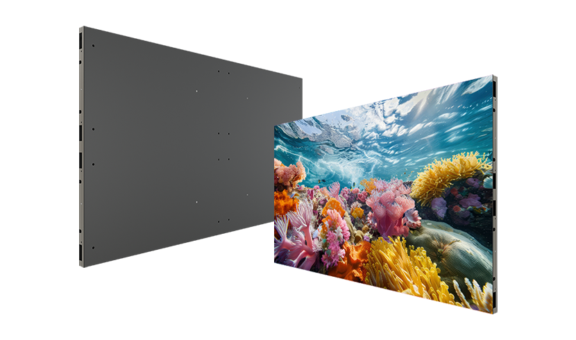
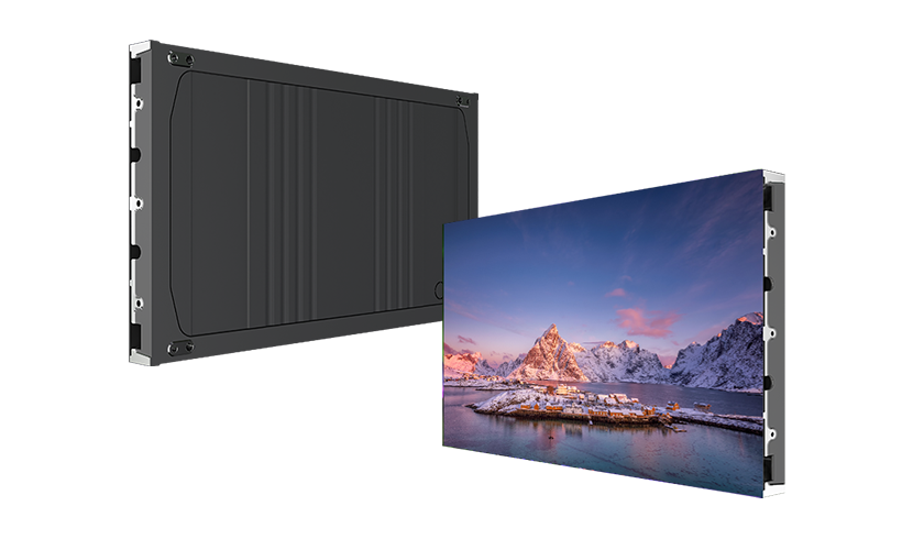
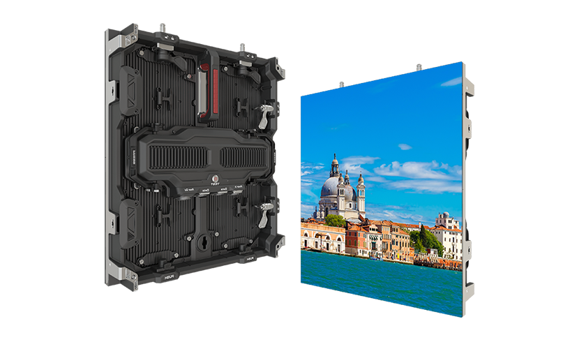
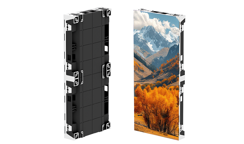
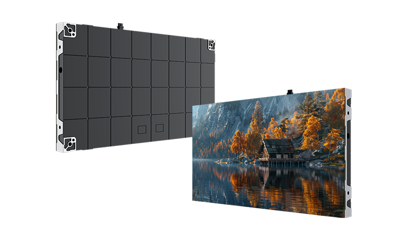
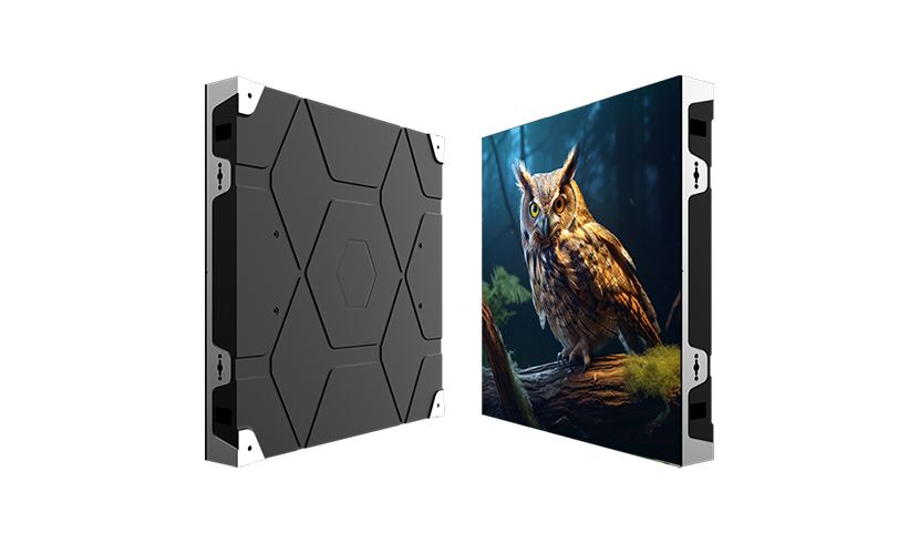
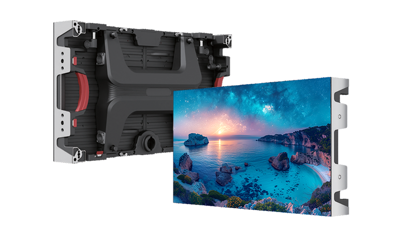
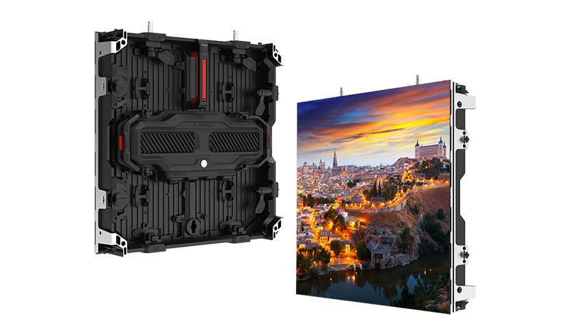
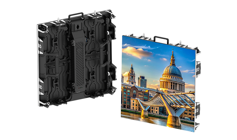
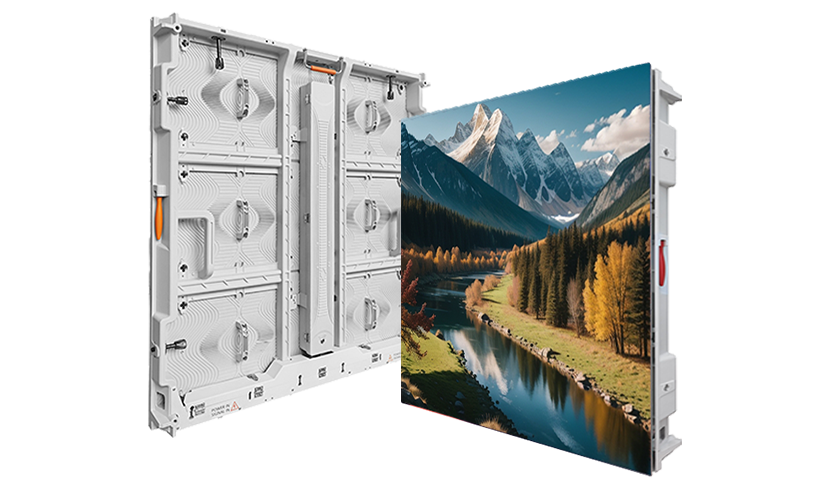
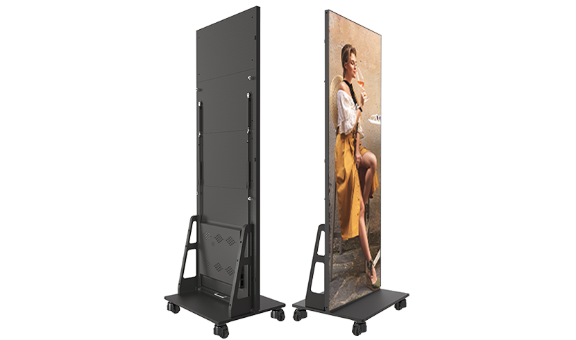
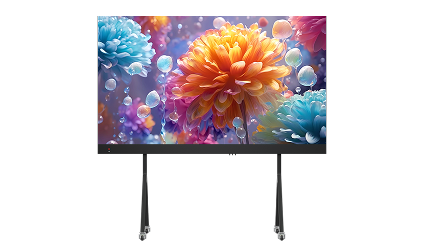
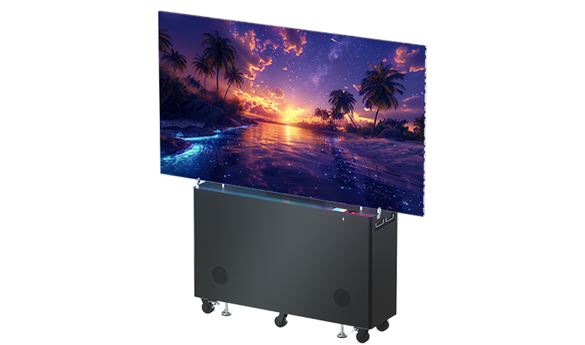
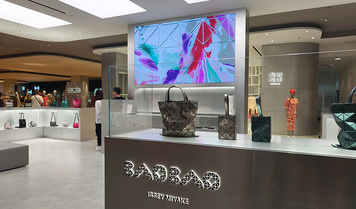
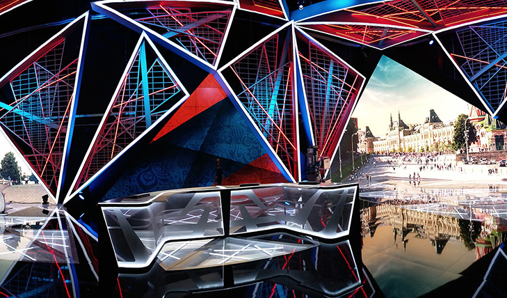
As a pioneer in the field of full flip chip display panels, LPDISPLAY has been deeply engaged in the realm of full flip chip technology and has achieved significant results. Why have we chosen to focus on this full flip chip process? This brings us to discuss the advantages of the full flip chip technology itself.
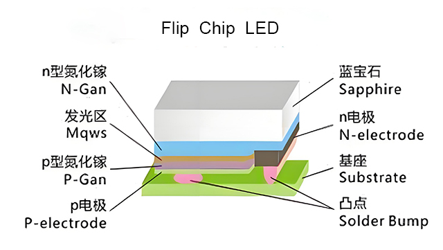
"Flip chip" refers to a technology that contrasts with traditional wire bonding methods. In traditional approaches, the electrical side of the chip connects to the substrate while facing upwards through metal wire bonding. In flip chip technology, the electrical side of the chip is oriented downwards, effectively turning the previous method upside down, hence the term "flip chip." The corresponding packaging process is termed "flip chip packaging." Flip chip LED packaging, which eliminates gold wire at the chip level, is based on flip chip technology. It reduces the gold wire bonding process found in traditional chip packaging, leaving only the chip paired with solder paste and phosphor for application.
Compared to formal chips, flip-chip technology has many advantages, including:
1. The flip chip process eliminates wire bonding, addressing issues that may arise in formal chip packaging, such as LED lights not lighting up, flickering, and significant light decay, which can be caused by poor bonding or contact with gold wires.
2. The chip and substrate are electrically and mechanically interconnected through solder paste, providing high bonding strength. The strength of the solder used in the flip chip process exceeds that of traditional gold wire bonding by more than 100 times.
3. Compared to the silver paste used in formal chip packaging processes, the solder paste used in flip chip technology offers superior heat dissipation performance.
4. The formal chip packaging process takes a longer time, with silver paste curing requiring more than 2 hours. In contrast, the flip chip process can reduce this time to 3-5 minutes, significantly improving production efficiency.
5. The formal chip packaging process is complex, making it impossible to repair a defective chip. In contrast, the flip chip process has a simpler application and allows for repairs when a chip is defective.
| Cost | Process complexity | Qualified yield | Reliability | Heat dissipation | Built-in ESD protection | |
| Formal chip LED | Low | Simple | Low | Normal | Bad | No |
| Flip chip LED | Middle | Complex | High | Excellent | Good | >6,000V(HKB), easy to implement |
The comparison diagram of formal chip packaging and flip chip packaging
With the development of miniaturization and reduced spacing, the flip chip process has gained attention in the industry due to its advantages. The gold wire in formal chip packaging limits the design of micro-spacing, as the shading ratio of its electrodes to the gold wire and the increased thermal resistance can reduce light efficiency and lifespan. The emergence of flip chips addresses the challenges faced by traditional packaging. Flip chip has no obstructions on the light-emitting surface, with electrodes flat on the pads, offering advantages such as better heat dissipation, higher light efficiency, and longer lifespan, making them suitable for micro-LED designs.

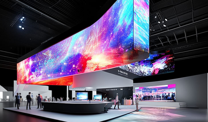
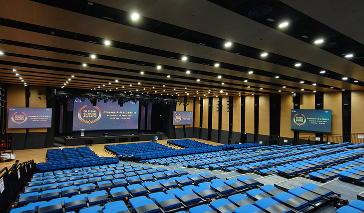
We will continue to innovate and develop in the field of full flip chip display, gain deeper insights into consumer needs, and provide more competitive and reliable high-definition LED small-pitch, visualization display technologies, and products in the big data information sector. We will consistently launch higher quality, more efficient, and smarter LED display solutions.


 中文
中文 日本語
日本語 Русский
 Español
 Deutsch
 français
 اللغة العربية